The ECG Circuit
An Electrocardiogram (ECG) device is designed to detect and enhance faint electrical signals generated by the heart, allowing medical professionals to analyze them for diagnostic purposes. As the incoming signals are relatively weak, in the range of millivolts (0.001 to 100 mV according to [1]), the ECG device needs to amplify them to a level that can be effectively processed by a microcontroller. Additionally, the device must employ adequate filtering techniques to remove unwanted noise from the signal; it is recommended to neglect frequencies exceeding a 0.05 to 100 Hz range. Another important consideration is the presence of a direct current (DC) component of approximately 500 mV due to contact between the electrodes and the patient’s skin [2].
12 Lead ECG System
The 12-lead ECG system is a method of measuring the electrical activity of the heart using four electrodes placed on each of the limbs and six on the chest. From the limb electrodes, an extra virtual electrode, called the Wilson’s central terminal (VCT), is created by averaging the signals from the two electrodes on each arm and one on the left leg. This central terminal is used as a reference point for the six electrodes on the chest. Another three leads, called the augmented limb leads, measure the potential difference between the limb electrodes and the Wilson’s central terminal. All the 12 leads can be seen in [3].
Components
Instrumentation Amplifier
The instrumentation amplifier is chosen as a safer alternative to measure the potential difference between electrodes to avoid causing discomfort to the patient. This is due to its ideally infinite input impedance, drawing a negligible amount of current from the patient’s body.

A schematic of the instrumentation amplifier [4] is presented in figure 1. The power supplies are ignored for simplicity. The use of the Op-Amps at the input terminals ensure that almost no current is extracted from the sample. The resulting signal is then fed into a standard differential amplifier.

Gain Calculation
For simplicity, we will assume that all resistances have the same value of $R$ except for $R_g$. As for ideal Op-Amps no current flows on the input ends, a KVL across path P1 highlighted in magenta on the figure 1 yields:
\begin{equation}\label{eq_r_g} V_1 - R_g I - V_2 = 0 \implies R_g I = V_1 - V_2 \end{equation}
As the current along the path P2 highlighted in orange on the figure 1 is the same since the bifurcations are met against the inputs of Op-Amps, we have that the KVL along this curve is:
\[V_\mathrm{out} + R I + R I + (2 R I + R_g I) - R I - R I = 0 \implies V_\mathrm{out} = -(2 R I + R_g I)\].
Replacing $I$ with equation \eqref{eq_r_g}
\[V_\mathrm{out} = -(2R + R_g)(V_1 - V_2)/R_g = (2R/R_1 + 1)(V_2 - V_1)\].
That is, the gain of this amplifier is entirely controlled by $R_g$ if all the resistances are kept the same. For this design, this gain factor can be chosen within the range of 51 to 101 to account for the different scales of the signals.
Band Pass Filter
Once the signal is captured by the instrumental amplifiers, we still have to filter out the incoming noise and DC component due to the contact between the electrodes and the patient’s skin. Both of these tasks can be accomplished with the use of a band pass filter, which allows only a certain range of frequencies to pass through. Typically, a Notch filter is also included to remove the 50/60 Hz noise caused by the power grid, but this model assumes that the input power is already stabilized a priori, as there are some situations where the signal will have meaningful components around this range [2]. There are many ways to design a band pass filter, the one presented the figure 1, which was obtained on [5], is called an Inverting Band Pass Filter. The reason for such a name becomes apparent when we calculate the transfer function of the system.
Transfer Function Calculation
To start, the parallel RC combination at the top of the circuit can be easily calculated with the use of the equivalent impedance $Z_2$ of a parallel circuit:
\[Z_2 = 1/(1/R_2 + 1/Z_{C_2})\]In here, $Z_{C_2}$ is the impedance of the capacitor $C_2$, which is just $1/(s C_2)$.
Doing a KVL path from the input $V_\mathrm{in}$ to the ground while passing through the input terminals of the Op-Amp, we have:
\begin{equation}\label{eq:band_filter_current} V_\mathrm{in} - R_1 I - Z_{C_1} I = 0 \implies I = V_\mathrm{in}/(R_1 + Z_{C_1}) \end{equation}
The reason I chose only a single symbol for the current $I$ is that the ideally infinite impedance of the inverting input of the Op-Amp ensures that the current won’t split between the two branches.
Another KVL also starting from $V_\mathrm{in}$ and passing through $R_1$, $C_1$, the parallel $R C$ until $V_\mathrm{out}$ yields:
\[V_\mathrm{in} - R_1 I - Z_{C_1} I - Z_2 I = V_\mathrm{out} \implies V_\mathrm{out} = - Z_2 I\]Replacing the current with the result found in equation \eqref{eq:band_filter_current}, we have:
\[V_\mathrm{out} = - V_\mathrm{in}\frac{Z_2}{R_1 + Z_{C_1}} = - V_\mathrm{in}\frac{1}{(1/R_2 + 1/Z_{C_2})(R_1 + Z_{C_1})}\]The minus signal at the output is an indication that the signal is inverted. Replacing the capacitor impedances with their respective expressions, the transfer function of the circuit $V_\mathrm{out}/V_\mathrm{in}:=H$ becomes:
\[H(s) = -\frac{s C_1 R_2}{(1 + s R_2 C_2)(1 + s C_1 R_1)}\]The RC combinations in the transfer function stand for the inverse of the frequency thresholds of the circuit. A more comprehensive analysis can be done by reducing the number of variables by letting $R_1 C_1 = 1/\omega_1$, $R_2 C_2 = 1/\omega_2$, and $R_2 = r R_1$.
\begin{equation}\label{eq:transfer_function_pretty} H(s) = -\frac{r s \omega_2}{(\omega_2 - \omega_1)} \left(\frac{1}{\omega_1 + s} - \frac{1}{\omega_2 + s}\right) \end{equation}
An important edge case is when $s = 0$, corresponding to an wave of zero frequency, or a DC signal. For this case, the transfer function is zero, meaning that the filter excludes DC signals as a natural consequence of its design.
Input Referred-Noise
Input referred noise models rely on the superposition principle, modelling the noisy output signal as a sum of the ideal output plus a noisy source caused by the components. With this idea, the output noise is calculated by adding various noise sources in the circuit, and assuming that no external input is present. To make calculations easier, each noise source is treated separately and then added together to obtain the total output noise.
Noise Model Instrumentation Amplifier
In the case of an instrumentation amplifier, the noise can be modelled in function of each of the three Op-Amps as in the figure [6].
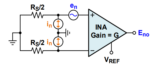
The mean squared contribution of the noise caused by the Instrumentation Amplifier ($E_\mathrm{no}^2$) is [6]
\begin{equation}\label{eq_ENO} \overline{E}_\mathrm{no}^2 = G^2 \Delta E (e_n^2 + 2 I_n^2 (R_S / 2)^2) \end{equation}.
In the equation \eqref{eq_ENO}, $G$ stands for the gain of the amplifier, $e_n$ is the voltage noise of the Op-Amp, $I_n$ is the current noise of the Op-Amp, and $R_S$ is the source resistance. The symbol $\Delta E$ is the noise equivalent bandwidth and is calculated as [6]
\[\Delta E= 1.57 \times \text{"INA Bandwidth"}(G)\]Noise Model Band Pass Filter
For the case of the band pass filter, we will make use of the Op-Amp noise model as presented in figure [7].
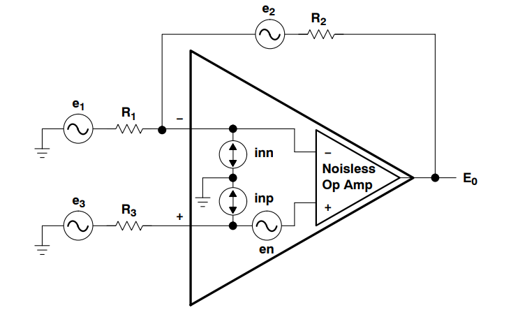
The topology of the circuit is similar to the band pass filter presented in the figure 1, with the exception that some of the resistances will have to be replaced by impedances. A conversion table between the two is presented in the table below (figure ).
| Noise Model | Band Pass Filter |
|---|---|
| $R_1$ | $Z_1 = R_1 + \frac{1}{s C_1}$ |
| $R_2$ | $Z_2 = \left(\frac{1}{R_2} + s C_2\right)^{-1}$ |
| $R_3$ | 0 |
Making the appropriate variable changes in the total mean square noise voltage of the Op-Amp ($E_\mathrm{filter}^2$) as presented in [7], we have:
\begin{equation} \label{eq_noise_filter} \end{equation}
\[\overline{E}^2_\mathrm{filter} = \frac{1}{2\pi} \mathrm{abs}\left(\int \mathrm{d} \omega \left( \overline{E}^2_\mathrm{no} \left( \frac{Z_2(i \omega)}{Z_1(i \omega)} \right)^2 + \overline{e_2}^2 + \overline{e_n}^2 \left(1 + \frac{Z_2(i \omega)}{Z_1(i \omega)} \right)^2 + \overline{I}_\mathrm{nn}(Z_2^2(i \omega)) \right)\right)\].
Where $Z_1$ and $Z_2$ are the respective impedances presented in figure 5. A little bit of algebraic manipulation reveals that the ratio $Z_2/Z_1$ is simply equation \eqref{eq:transfer_function_pretty} without the minus sign. So, we can further simplify equation \eqref{eq_noise_filter} as:
\[{\overline{E}_\mathrm{filter}}^2 = \frac{1}{2\pi}\left(\int \mathrm{d} \omega ({\overline{E}_\mathrm{no}}^2 H^2(i \omega) + \overline{e_2}^2 + \overline{e_n}^2 (1-H(i \omega))^2 + {\overline{I}_\mathrm{nn}} Z_2^2(i \omega))\right)\]Rearranging:
\[{\overline{E}_\mathrm{filter}}^2 = \frac{1}{2\pi} \mathrm{abs}\left(\int \mathrm{d} \omega (({\overline{E}_\mathrm{no}}^2 + \overline{e_n}^2) H^2(i \omega) + (\overline{e_2}^2 + \overline{e_n}^2) - 2\overline{e_n}^2H(i \omega) + {\overline{I}_\mathrm{nn}} Z_2^2(i \omega))\right)\]In the worst case scenario, this integral is bounded by the triangle inequality:
\[{\overline{E}_\mathrm{filter}}^2 \leq \frac{1}{2\pi} \int \mathrm{d} \omega \left(({\overline{E}_\mathrm{no}}^2 + \overline{e_n}^2) \mathrm{abs}(H(i \omega))^2 + (\overline{e_2}^2 + \overline{e_n}^2) + 2\overline{e_n}^2 \mathrm{abs}(H(i \omega)) + {\overline{I}_\mathrm{nn}} \mathrm{abs}(Z_2(i \omega))^2 \right)\]In which I have assumed that all the voltage and current noise sources aren’t complex. Now, we will abuse the boundedness of the $\mathrm{abs}(H(i \omega))$ and $\mathrm{abs}(Z_2(i \omega))$ functions to use the ML inequality:
\begin{equation}\label{eq_noise_upper_bound}\end{equation}
\[{\overline{E}_\mathrm{filter}}^2 \leq \frac{\Delta \omega}{2\pi} \left(({\overline{E}_\mathrm{no}}^2 + \overline{e_n}^2)\left(2r \frac{\omega_2}{\omega_2 - \omega_1}\right)^2 \ + (\overline{e_2}^2 + \overline{e_n}^2) \ + 2( \overline{e_n}^2) \left(2r \frac{\omega_2}{\omega_2 -\omega_1}\right) + R_2 {\overline{I}_\mathrm{nn}} \right)\].
The term $\Delta \omega$, not to be confused with $\omega_2 - \omega_1$, stands for the noise bandwidth of the Op-Amp in rad/s. Equation \eqref{eq_noise_upper_bound} with the definition of ${\overline{E}_\mathrm{no}}$ equation \eqref{eq_ENO} provide a maximum upper bound to the output noise caused by the conjuction of the instrumentation amplifier and the band pass filter.
Since all the $\overline{e_j}$ factors have a $k_B T$ term for noise due to thermal agitation, stabilizing the circuit’s temperature with coolers will help with noise reduction.
- [1]W. Y DU, “Design of an ECG Sensor Circuitry for Cardiovascular Disease Diagnosis,” International Journal of Biosensors & Bioelectronics, vol. 2, no. 4, May 2017, doi: 10.15406/ijbsbe.2017.02.00032.
- [2]K. L. Venkatachalam, J. E. Herbrandson, and S. J. Asirvatham, “Signals and Signal Processing for the Electrophysiologist: Part I: Electrogram Acquisition,” Circulation: Arrhythmia and Electrophysiology, vol. 4, no. 6, pp. 965–973, Dec. 2011, doi: 10.1161/circep.111.964304.
- [3]J. Malmivuo and R. Plonsey, “Bioelectromagnetism. 15. 12-Lead ECG System,” 1975, pp. 277–289.
- [4]“The Differential Amplifier.” [Online]. Available at: https://www.electronics-tutorials.ws/opamp/opamp_5.html.
- [5]“Active Band Pass Filter.” [Online]. Available at: https://www.electronics-tutorials.ws/filter/filter_7.html.
- [6]“Operational Amplifiers: Noise Calculations of Instrumentation Amplifier Circuits.” [Online]. Available at: https://www.renesas.com/us/en/document/apn/r13an0011-noise-calculations-instrumentation-amplifier-circuits-rev100.
- [7]“Noise Analysis in Operational Amplifier Circuits.” [Online]. Available at: https://www.ti.com/lit/an/slva043b/slva043b.pdf?ts=1706030563174&ref_url=https%253A%252F%252Fsearch.brave.com%252F.